The N40 Android smart PDA features a Cortex-A53 qu...
Explore an innovative Personal Digital Assistant f...
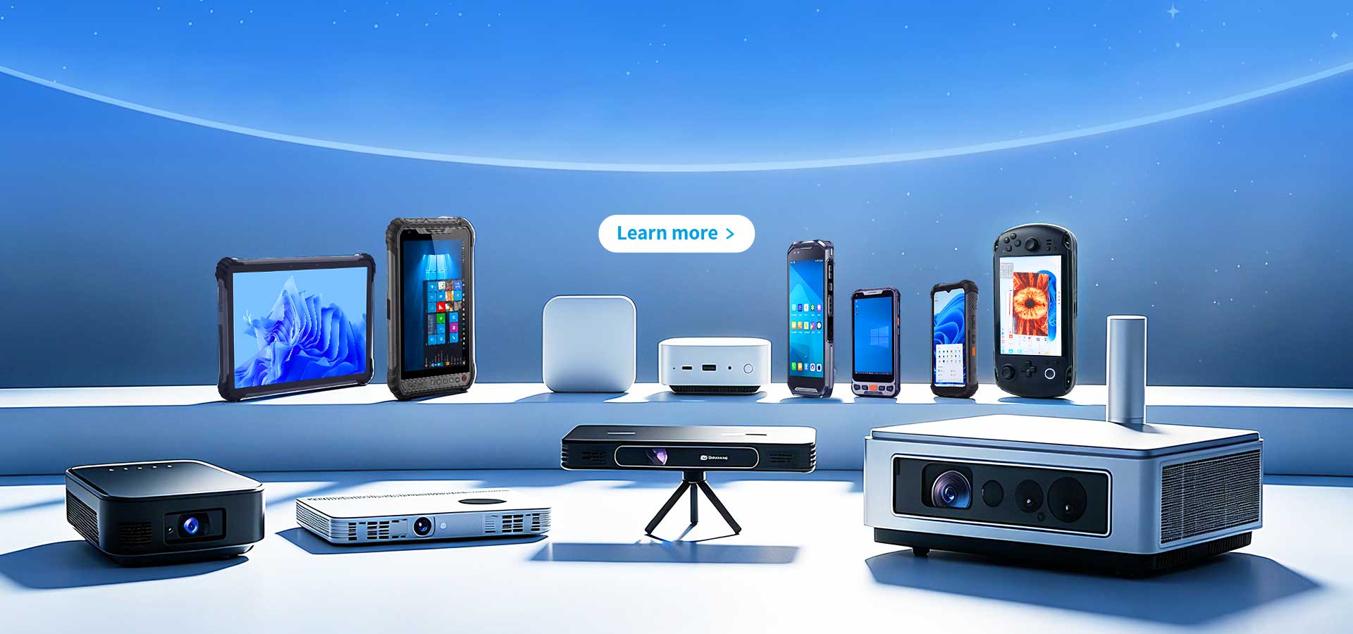
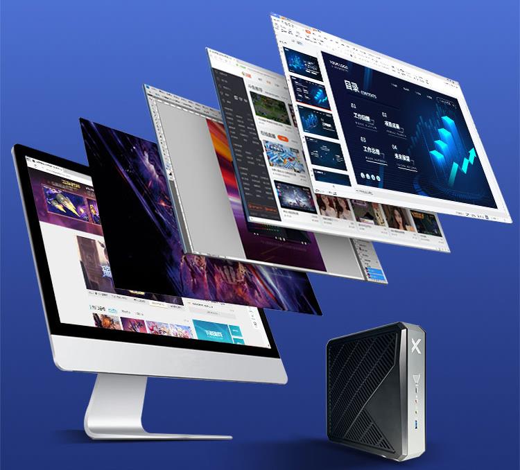
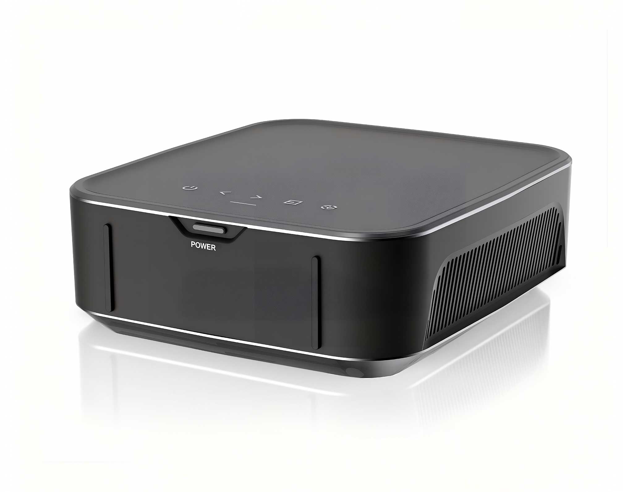
One Device, Dual Functions – A Projector and a Com...
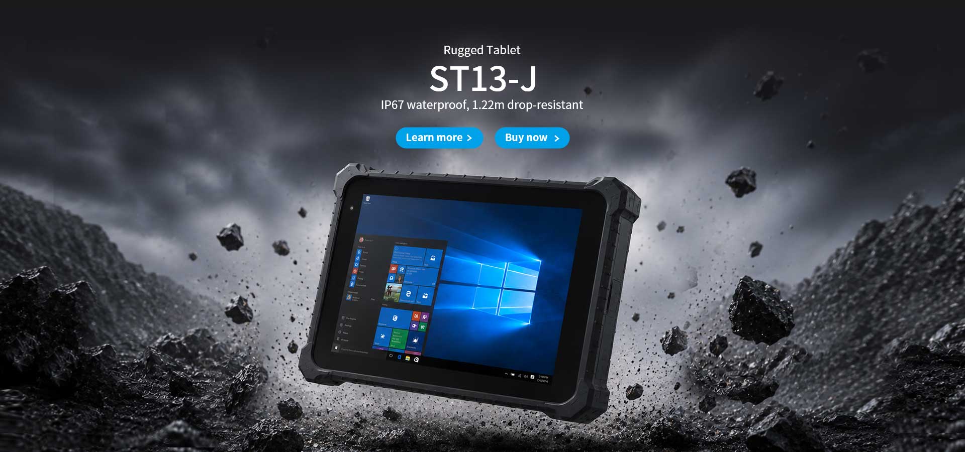
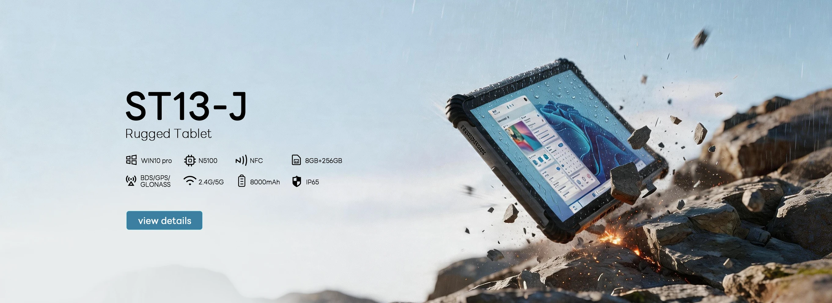
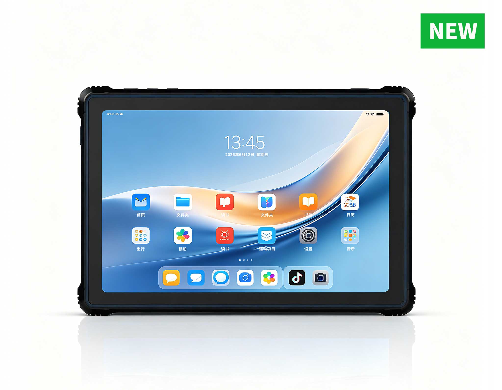
RT81 4G Rugged Tablet | 10.1" FHD 400nit | Qu...
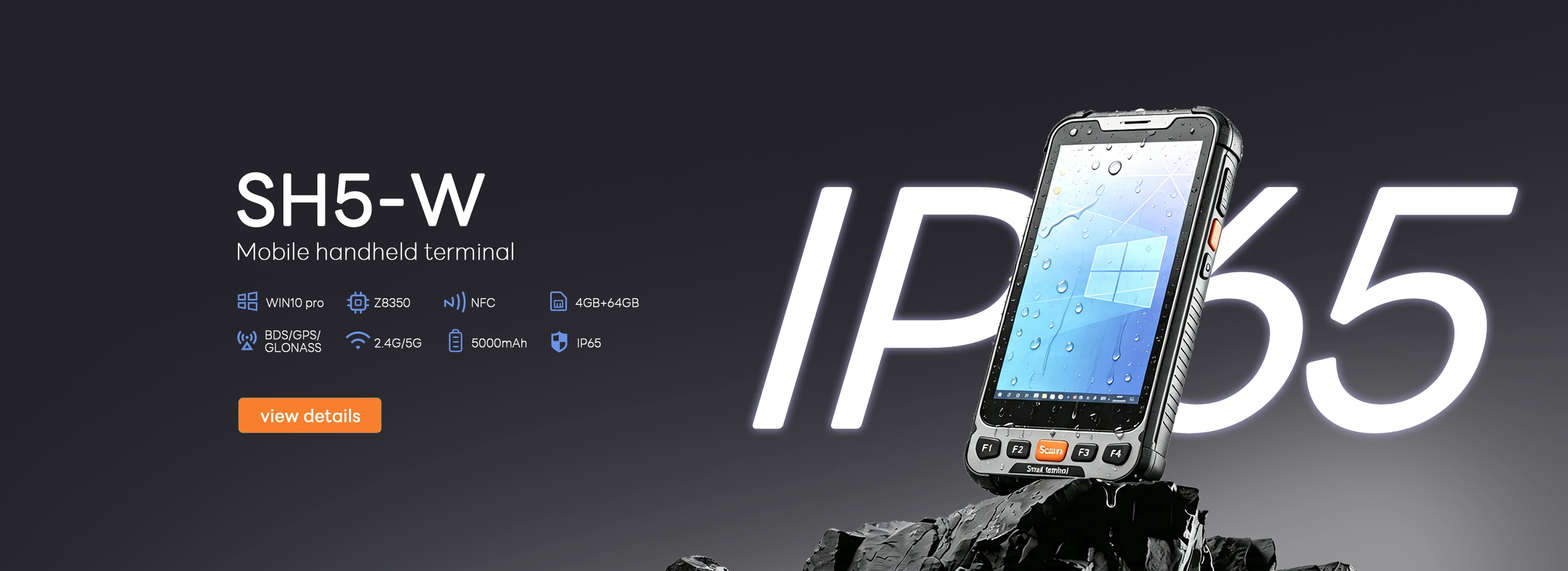
RS50 5G Rugged Handheld Terminal | 6.3" FHD+ ...
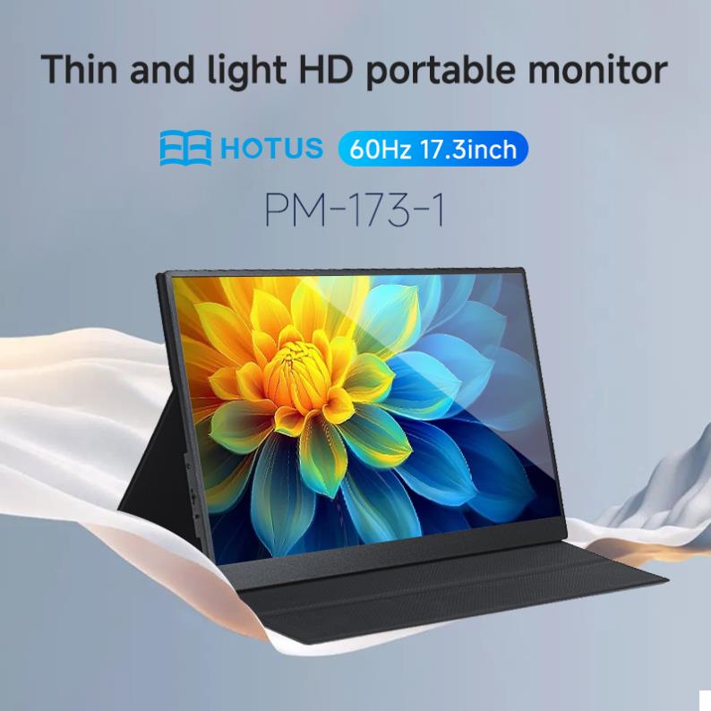
The PM156-1 is a 15.6-inch portable PC monitor fea...
Full SpecificationsModelHotus ST9‑MOSWindows 10/11...
")
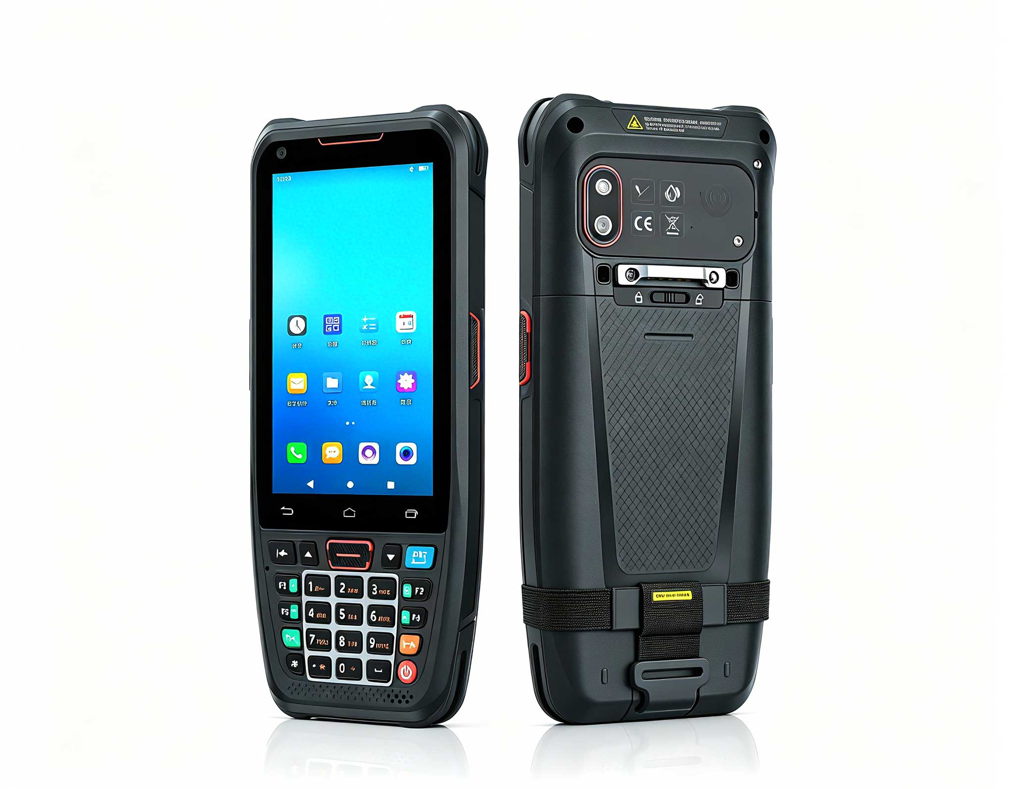
Hotus F502 — RFID PDA for semiconductor fab WIP tracking
")
By HOTUS Technology | April 2026
The numbers are staggering. According to Deloitte‘s 2026 Global Semiconductor Industry Trends Report, global semiconductor sales are projected to reach $975 billion in 2026, a 26% increase from 2025‘s 22% growth [citation:7]. By 2036, annual sales are expected to surpass $2 trillion. But beneath this headline lies a structural anomaly: high‑value AI chips contribute approximately half of total revenue yet account for less than 0.2% of unit shipments [citation:7]. While AI chips soar, semiconductors for automotive, smartphones, and non‑data‑center communications are growing at a much slower pace.
This asymmetry is reshaping the entire semiconductor supply chain. Memory revenue alone is expected to hit $200 billion in 2026 — 25% of the total market — driven by demand for HBM3, HBM4, and DDR7 [citation:7]. The insatiable appetite for AI training and inference has led to a “zero‑sum game” for wafer and packaging capacity, driving up prices for consumer memory (DDR4/DDR5) by approximately four times between September and November 2025, with further increases of up to 50% expected in the first half of 2026 [citation:7].
For semiconductor manufacturers, this boom is both an opportunity and a crisis. Fab utilization is at record highs. Cycle times are under pressure. And the cost of a single misprocessed wafer — or a misplaced lot — has never been higher. This is where rugged mobile computing enters the picture.
")
A modern semiconductor fab is one of the most complex manufacturing environments on Earth. Hundreds of processing steps. Dozens of tools. Thousands of wafer lots moving through the facility at any given moment. A single mis‑routed lot can delay an entire production schedule by weeks. A mis‑identified wafer can trigger a costly rework — or worse, a recall.
Traditional paper‑based tracking systems and consumer mobile devices are inadequate for this environment. Fabs require cleanroom‑compatible, chemically resistant, glove‑friendly mobile computers that can withstand frequent sanitization, operate in static‑sensitive areas, and integrate seamlessly with manufacturing execution systems (MES).
The Hotus F502 RFID Barcode Scanner PDA and Hotus ST11‑M 10.1″ Windows Rugged Tablet are purpose‑built for semiconductor manufacturing environments.
The F502 PDA combines UHF RFID and high‑performance barcode scanning in a single rugged device. In a semiconductor fab, this capability is transformative:
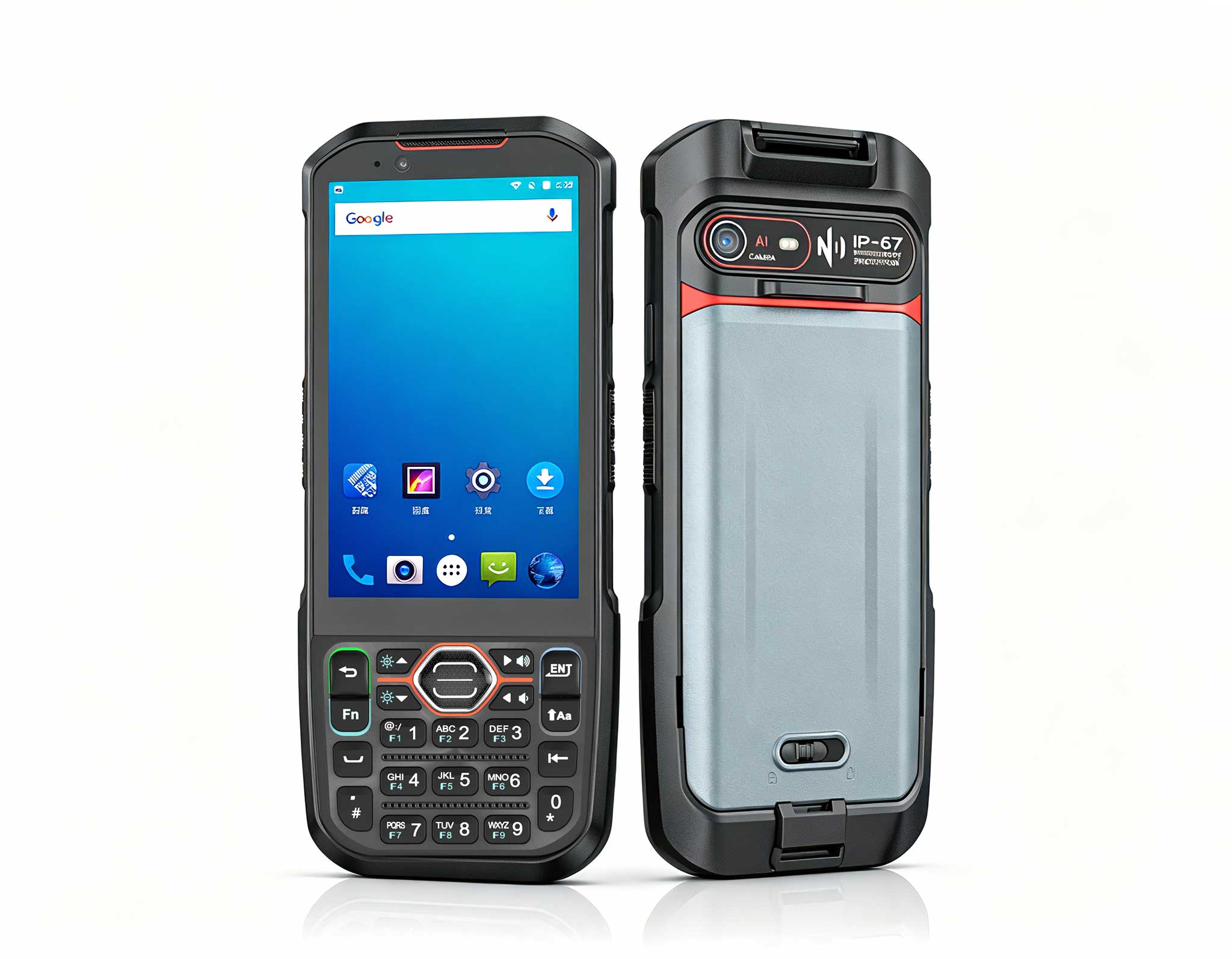
The ST11‑M Windows tablet serves as the mobile interface for fab supervisors and quality engineers. With its sanitizable IP67‑rated housing, it can be used on the cleanroom floor without contamination risk. The high‑brightness display remains readable under the intense lighting of a fab cleanroom, and the glove‑compatible touchscreen works with cleanroom gloves.
The semiconductor industry‘s structural shift toward AI chips has profound implications for manufacturing. AI chips are larger, more complex, and more expensive than standard logic or memory chips. A single high‑end AI processor can cost tens of thousands of dollars. The margin for error is effectively zero.
Moreover, AI chip customers — cloud providers and AI infrastructure companies — demand complete traceability from wafer to finished device. They want to know which fab produced the wafer, which tools processed it, which operators handled it, and what test results were recorded at each step. Meeting these demands requires digital, auditable, real‑time data capture — exactly what rugged mobile devices provide.
According to Deloitte‘s report, the industry is rapidly shifting toward system‑level performance optimization rather than just transistor scaling [citation:7]. Chiplet technology is being widely adopted to improve yield and energy efficiency. HBM memory is being integrated directly alongside logic chips to achieve TB/s data transfer speeds. Co‑packaged optics (CPO) are expected to see widespread adoption in 2026, reducing power consumption by 30-50% while improving bandwidth efficiency [citation:7]. These advanced packaging techniques require even tighter coordination between manufacturing steps — and even greater reliance on robust mobile data capture.
The scale of investment is breathtaking. According to the National Bureau of Statistics, high‑tech manufacturing investment grew 5.2% year‑over‑year in Q1 2026, with electronics and communications equipment manufacturing investment up 6.6% [citation:9]. Emerging sectors like embodied intelligence and 6G are rapidly becoming new engines of investment growth [citation:9].
Deloitte notes that strategic alliances between AI, semiconductor, and cloud infrastructure providers are reshaping the industry [citation:7]. “Circular financing” models — where chip companies invest in AI startups, which in turn become customers — are creating vertically integrated ecosystems. As capital and computing resources flow in both directions, the demand for edge computing infrastructure — rugged tablets and PDAs — grows in lockstep.
A leading logic semiconductor manufacturer deployed 200 F502 PDAs and 50 ST11‑M tablets across its 300mm wafer fab. Results after 12 months:
")
Hotus ST11‑M — sanitizable Windows tablet for fab quality and traceability
Contact HOTUS Technology to discuss your semiconductor manufacturing needs, request pilot units, or explore custom RFID PDA and sanitizable Windows tablet solutions for high‑volume fab operations.