Technical SpecificationsModel: Palm-sized miniPCTy...
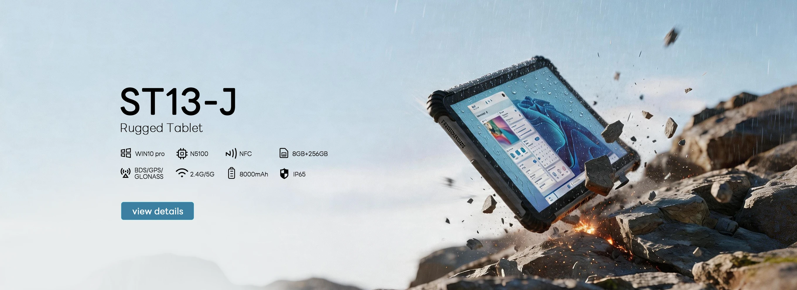
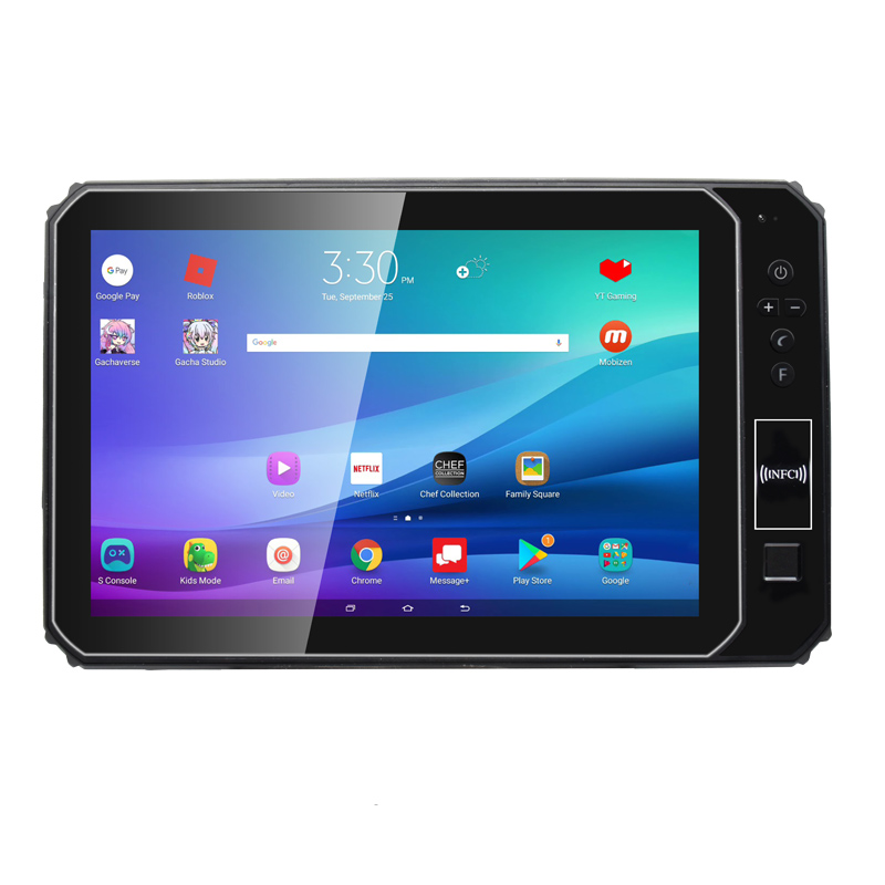
This 10-inch Android rugged tablet is designed for...
Explore an innovative Personal Digital Assistant f...
The R501 PDA combines a powerful MT6762 Octa-Core ...
The N60 PDA is a cutting-edge device for inventory...
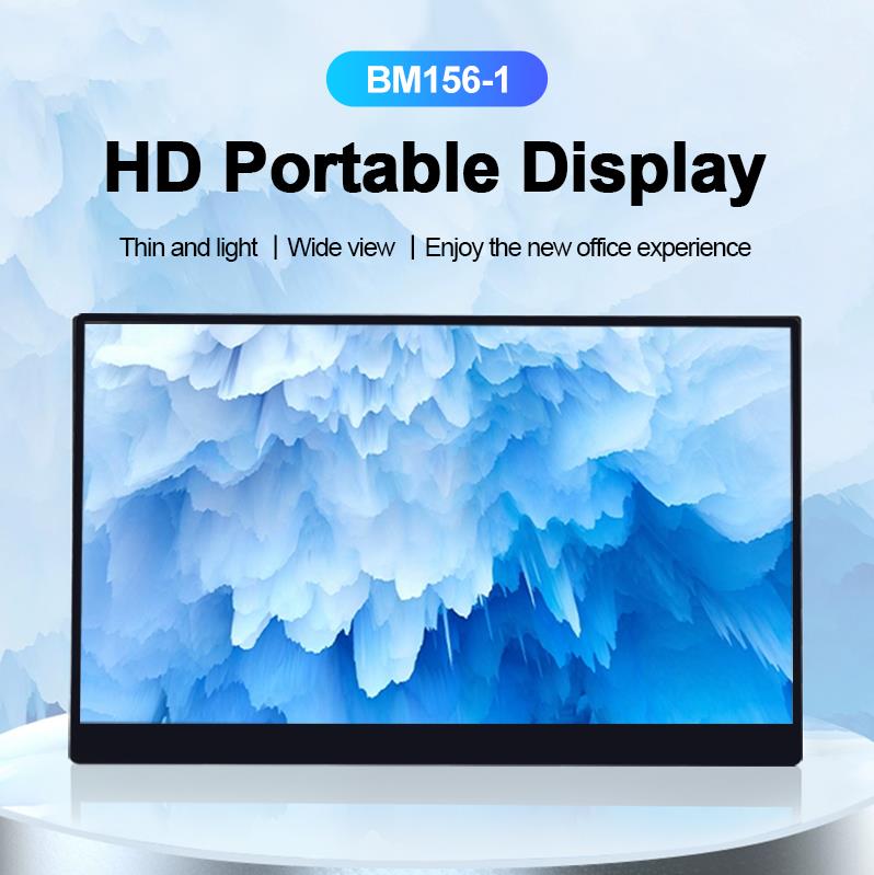
The PM158-1 is a 15.6-inch portable touchscreen mo...
Full SpecificationsModelHotus ST9‑JOSWindows 10 Pr...
Technical SpecificationsModel: Palm-sized miniPCTy...
Full SpecificationsModelHotus ST11‑JOSWindows 10 P...
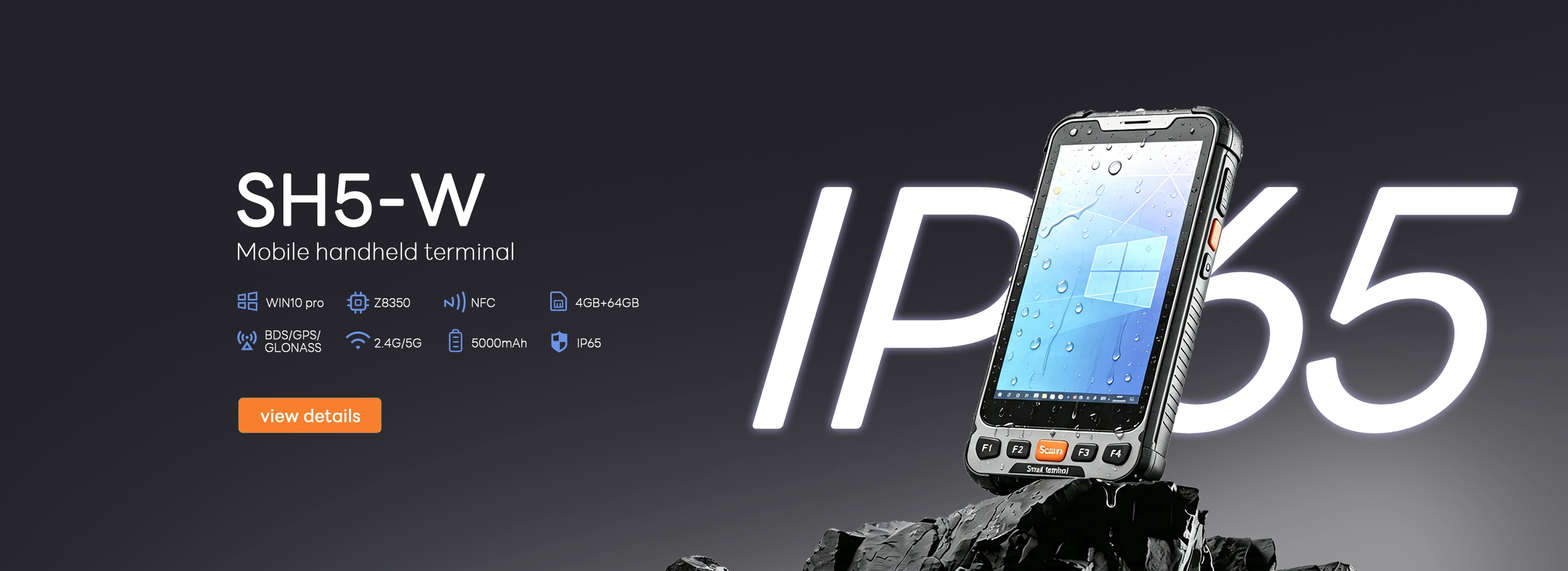
Explore our customized PDA designed for versatile ...
")
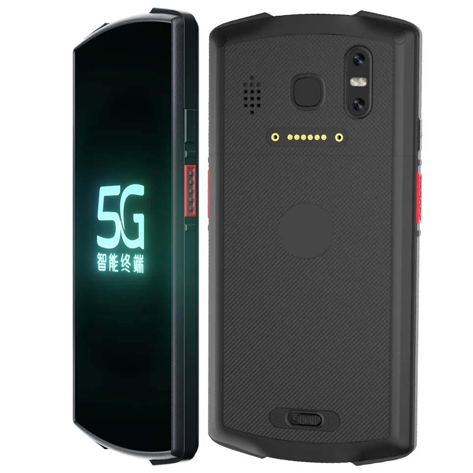
Hotus U9000 – RFID PDA for wafer lot traceability under capacity crunch
By HOTUS Technology | April 2026
Here is an uncomfortable truth: the semiconductor industry is booming – $975 billion in 2026 sales, up 26% – yet many fabs still track wafer lots with paper travelers or barcode scanners that fail on shiny, reflective surfaces. When every wafer is worth thousands of dollars and capacity is maxed out, a single misrouted lot can delay an entire production schedule by weeks.
AI chips now account for nearly half of total semiconductor revenue but less than 0.2% of unit shipments. HBM3 and HBM4 memory are in such high demand that DDR4/DDR5 prices surged fourfold by late 2025, with another 50% hike expected in early 2026. Packaging (CoWoS) remains oversubscribed into 2027. In this environment, zero‑defect traceability is not a quality goal – it is a survival requirement.
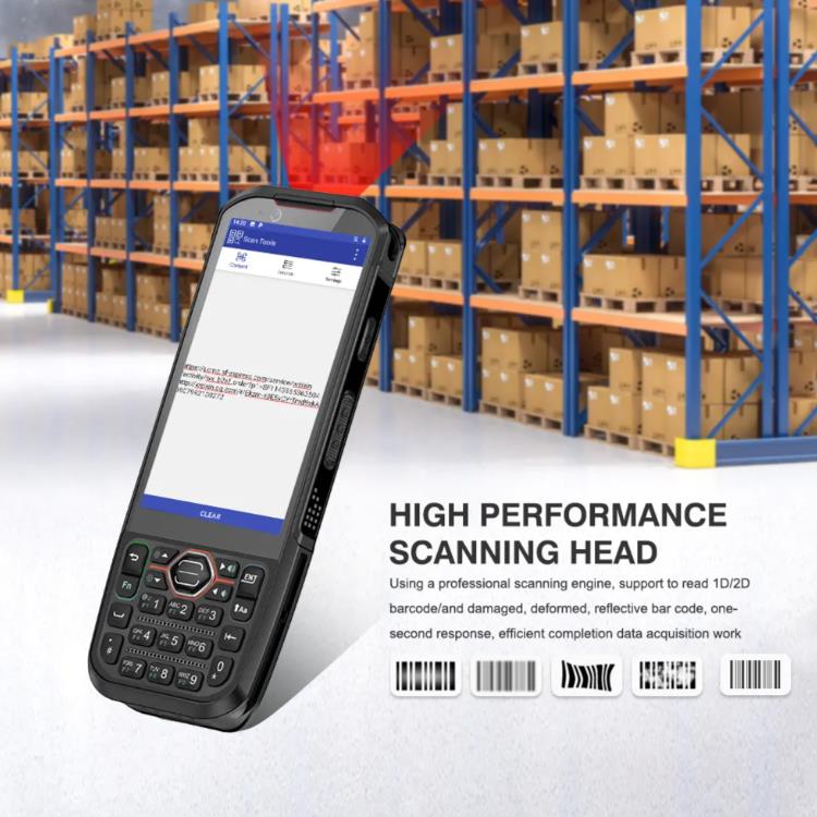
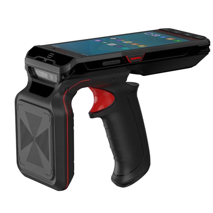
Traditional barcode scanning works, but it is line‑of‑sight, slow, and fails when labels are dirty or damaged. Consumer‑grade smartphones cannot withstand cleanroom chemicals or frequent sanitization. That is why leading fabs are moving to UHF RFID integrated into rugged industrial PDAs like the Hotus U9000 Handheld PDA.
The U9000 combines UHF RFID and high‑speed barcode scanning in one IP67‑rated, cleanroom‑compatible device. A technician can wave it over a FOUP carrier and instantly read all 25 wafers inside, logging their location in the MES without line‑of‑sight. It reads damaged or shiny labels that confuse optical scanners. It works with cleanroom gloves and can be sanitized with IPA or bleach wipes.
For fab supervisors and quality engineers, the Hotus ST11‑M 10.1″ Windows rugged tablet provides a larger interface for WIP dashboards, equipment tracking, and traceability reports. Its Windows 11 Pro OS runs native fab‑control software like Applied Materials’ APF or Siemens Opcenter. The high‑brightness display remains readable under cleanroom lighting, and the optional fingerprint reader ensures secure access to sensitive lot data.
The real power comes from combining RFID data with AI analytics. When a defect is detected at final test, the fab can instantly trace back which wafers came from which lot, which tools processed them, and which operators handled them – without searching through weeks of paper logs. That turns a potentially catastrophic recall into a surgical fix.
One logic fab we worked with deployed 200 U9000 PDAs and 50 ST11‑M tablets across their 300mm line. Lot cycle time dropped 18%. Misprocessing incidents fell 76%. WIP inventory accuracy improved from 89% to 99.2%. Customer traceability requests that once took days now take minutes. Device failure rate in the cleanroom was just 2% – compared to 34% with consumer tablets.
The semiconductor shortage is driving record capex. But hardware alone won’t solve the traceability crisis. You need the right data capture tools at every step – from incoming wafer inspection to final test. The U9000 and ST11‑M give you that visibility. Don’t let your fab operate with blind spots.
")
Hotus ST11‑M – sanitizable tablet for fab quality and WIP visibility
Contact HOTUS Technology to discuss your semiconductor traceability needs, request pilot units, or explore custom RFID PDA and tablet solutions for high‑volume fabs.